Building brick by brick is obsolete. Research Professor Sergei V. Kalinin wants to construct materials atom by atom.
Kalinin is the 2022 recipient of the Foresight Institute’s prestigious Feynman Prize for Experiment, which recognizes researchers making exceptional strides in cutting-edge nanotechnology. The prize is named after American physicist Richard Feynman, who first put forth the idea of nanotechnology—the ability to study and alter materials on an atomic level—in 1959.
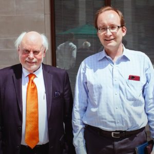
Sergei V. Kalinin (right) stands with Nobel Laureate Sir James Fraser Stoddart.
Previous winners in the Experiment category include Nobel Laureate Sir James Fraser Stoddart, who created the first molecular machine, and Michelle Simmons, who invented atomic-scale electronics.
“I feel extremely honored and humbled to receive the Feynman Experimental Prize,” said Kalinin, who will be the Department of Materials Science and Engineering (MSE) Weston Fulton Chair Professor starting in Spring 2023.
He gratefully acknowledged his colleagues at both UT and Oak Ridge NationalLaboratory (ORNL) for their dedication to his “fab on a beam” project, which would allow the analysis and fabrication (“fab”) of materials one atom at a time.
“We have shared this idea of electron beam matter assembly for almost a decade now,” Kalinin said. “This award recognizes the effort of multiple collaborators, whose joint efforts spanning machine learning, electronic engineering, and microscopy have brought it many steps closer to reality.”
Kalinin was inspired to pursue nanotechnology by the work of K. Eric Drexler, the American engineer who in 1991 proposed the idea of a nanoscale “assembler,” a microscopic machine which would be able to create a perfect copy of itself.
When Kalinin reached graduate school, MSE Professor Gerd Duscher introduced him to electron microscopy and—along with MSE Adjunct Professor Steve Pennycook—encouraged him to come work in the Knoxville area.
Currently, Kalinin’s research focuses on the applications of machine learning in microscopy. One of his goals is to make microscopes that can automatically identify interesting structures and configurations, then explore their functionality. Such microscopes could help reveal the fundamental mechanisms in energy storage and conversion and enable the discovery and investigation of autonomous materials (such as damage-sensing or self-healing polymers).
A scanning probe microscope (SPM) uses a tiny physical probe, like the needle on a record player, to visualize samples at the mesoscale, where objects are more than 10 nanometers wide (about 10,000 times thinner than a sheet of paper) and can obey both quantum and classical laws of physics. Kalinin uses an SPM to visualize three major physics phenomena on a molecular level: electrochemical reactions, ferroelectricity, and transport phenomena.
In an electrochemical reaction, chemical changes in a material influence the electrical potential of an external circuit (or vice versa), such as when a lithium-ion battery generates electrical power.
Ferroelectric materials do not conduct electricity, but the crystals in them spontaneously polarize in a single direction that can be flipped when an electric field is applied. This is similar to the polarization of a magnet, but the force at work is electric rather than magnetic.
Finally, transport phenomena include electronic and ionic transport, which underpin the functionality of solar cells, batteries, fuel cells, and novel neuromorphic computing devices (which are built to mimic biological brains).
Kalinin and his collaborators also use AI-driven scanning transmission electron microscopy (STEM) to study the physical properties of materials less than 0.2 nanometers wide (about one-tenth the width of a strand of DNA). STEM uses a fast-moving electron beam to visualize matter on an atomic level, unveiling the atomic-scale structure and fundamental mechanisms that govern a material’s functionality.
As it operates, the electron beam also induces reactions within the sample materials. Ultimately, Kalinin hopes to use those reactions to enable direct atomic assembly.
“It is a road of a thousand miles to make materials atom by atom at the needed scale,” Kalinin said, “but this is the road that leads to silicon compatible quantum computing, novel electronic and biological devices, nanorobotics for medicine and space exploration, and many applications we can only imagine now.”
In 63 years, nanotechnology has transformed from a thought experiment to a bustling discipline. Kalinin has earned his place in that story, but he is not finished yet.
“I am honored to be a part of the team that paved the road for these first steps,” he said. “I am looking forward to helping make the visions of Feynman, Drexler, and many visionaries and dreamers a reality.”